Cadence Pcb Layout
About the Author Cadence PCB solutions is a complete front to back design tool to enable fast and efficient product creation Cadence enables users accurately shorten design cycles to hand off to manufacturing through modern, IPC2581 industry standard.

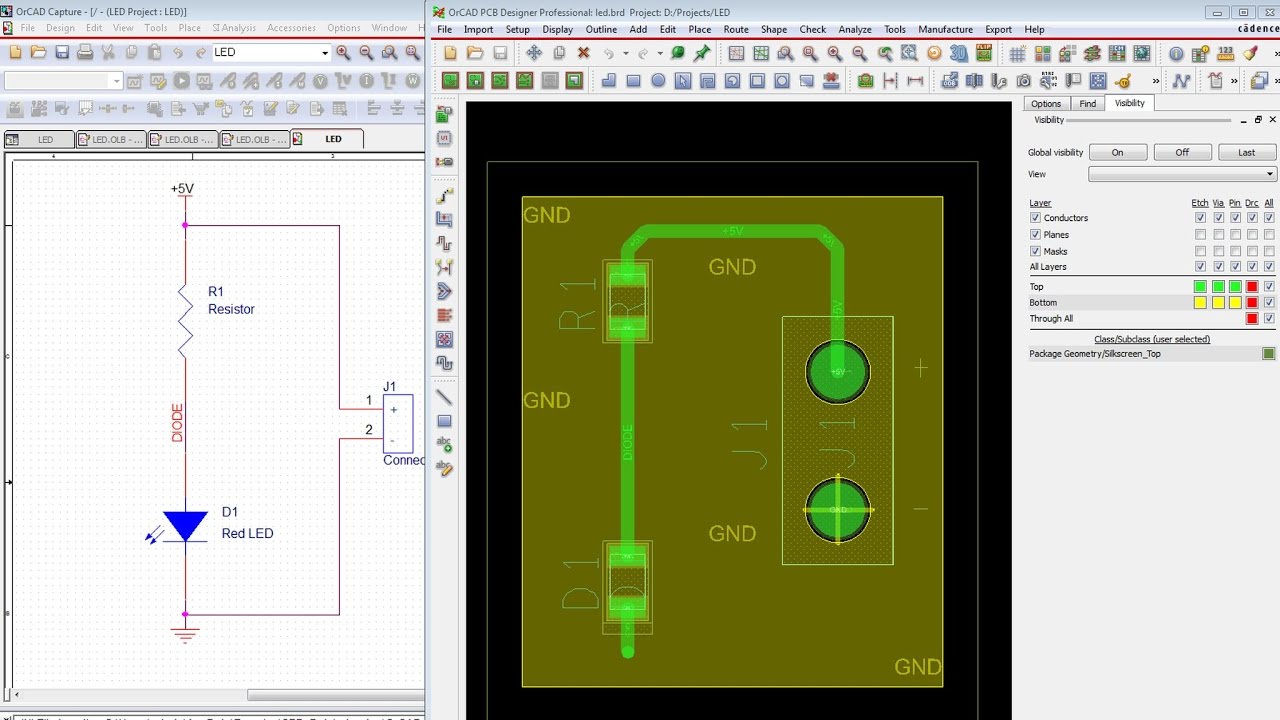
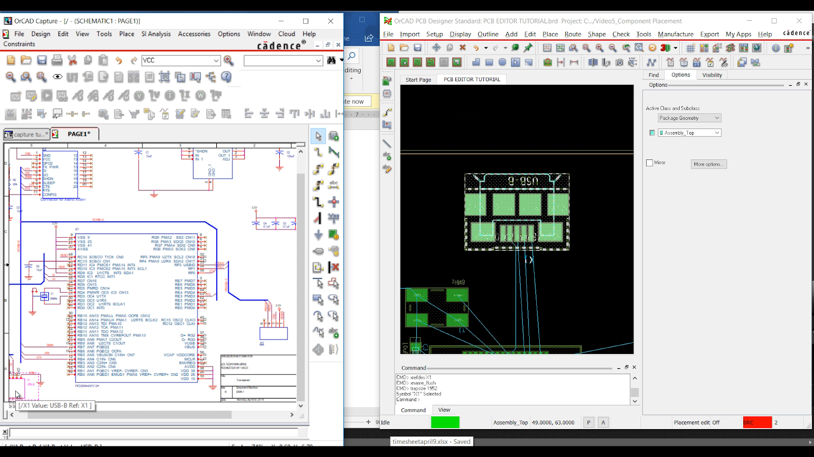
Cadence pcb layout. Enter the project name, specify the project placement path;. Cadence front end, PCB layout, and routing technology offers a scalable, easytouse, constraintdriven PCB design solution for simple to complex PCBs, including those with RF etch components It. PCB設計與分析 Cadence® PCB design solutions enable shorter, more predictable design cycles with greater integration of component design and systemlevel simulation for a constraintdriven flow.
Cadence PCB 2 hrs · As an environmentally friendly solution for consumer, military, medical, and industrial applications, paper circuit boards offer a glimpse of the future of # electronic products. Connecting pads, drawing tracks, placing VIAs, doing fanout, moving & sliding tracks, adding shapes, creating shortcuts Find the complete course at http//. We currently support the latest versions of the tool We are proud to be one of a handful of Early Adopter Program Members with Cadence.
Cadence PCB solutions is a complete front to back design tool to enable fast and efficient product creation Cadence enables users accurately shorten design cycles to hand off to manufacturing through modern, IPC2581 industry standard Follow on Linkedin Visit Website More Content by Cadence PCB Solutions. Like many of you, we've worked from home We juggled house and office work, washed our hands innumerable times a day, rinsed every grape before putting it in the fridge, and scrambled to look presentable in conference. This article brings you a detailed tutorial on cadence allegro PCB layout First, use Design Entry CIS (Capture) design schematic 1, create a project File–“new–“project;.
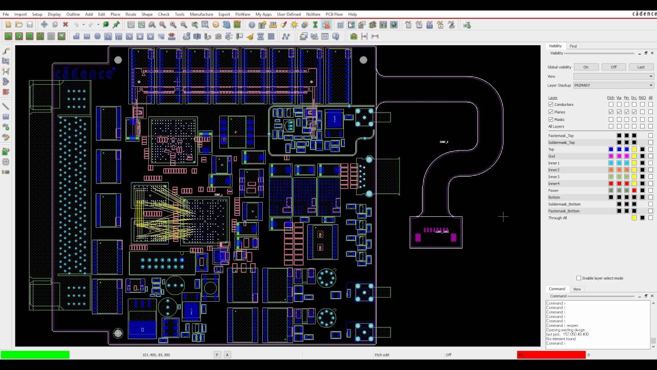
Customize Your PCB Design Experience with OrCAD new features like design reuse, advanced PCB routing technologies, Indesign DFM, Interactive 3D Canvas. You need the right tools to get a job done, and this is especially true in PCB design Here are some features that you should look for when evaluating your next set of # PCB layout tools https//bitly/3ioN5FD # cadence. Cadence PCB BackEnd Board Layout and Routing Better designers make better boards PCB Layout Allegro PCB Designer RigidFlex Once upon a time, PCB designers were draftsman The measure of their craft was twofold—quality of lines and speed of completion But designs have changed, and so have designers.
99 Cadence Allegro Pcb Layout Engineer jobs available on Indeedcom Apply to Design Engineer, Designer, Electrical Engineer and more!. Design a simple board in OrCAD and Allegro PCB Draw a schematic Route PCB Generate the essential files for PCB manufacturer Cadence software is very powerful During this course you will learn the basics of using Cadence software OrCAD and Allegro are professional software used to design the most advanced electronics boards. Cadence PCB solutions is a complete front to back design tool to enable fast and efficient product creation Cadence enables users accurately shorten design cycles to hand off to manufacturing through modern, IPC2581 industry standard Follow on Linkedin Visit Website More Content by Cadence PCB Solutions.
The Cadence® Allegro® PCB Editor helps bring your innovative and bleedingedge designs to life With a comprehensive, powerful and easytouse suite of tools, you can effortlessly simplest or most complex projects. PCB Design and Analysis Cadence® PCB design solutions enable shorter, more predictable design cycles with greater integration of component design and systemlevel simulation for a constraintdriven flow. PCB Design and Analysis Cadence® PCB design solutions enable shorter, more predictable design cycles with greater integration of component design and systemlevel simulation for a constraintdriven flow.
Here we run through a very simple example using the OrCAD tools We go from a blank schematic to a finished PCB output This is designed to help new users ge. A # PCB library can help you to use the parts you need without having to constantly reinvent the wheel with each new design you create Here are some ideas about how choosing the right component for your # circuit from a library can help with your next design https//bitly/3qALoYz # cadence See More. How to Design PCB Layout Rules That Work Here is how you can design PCB layout rules efficiently that will help you to lay out a board design without errors and be ready for manufacturing.
The only native, bidirectional connection between SOLIDWORKS and Cadence OrCAD and Allegro PCB Dassault 3DExperience The 3DExperience platform supports concepttoproduction with industry solution experiences based on 3D design, analysis, simulation, and intelligence software in a collaborative interactive environment. Customize Your PCB Design Experience with OrCAD new features like design reuse, advanced PCB routing technologies, Indesign DFM, Interactive 3D Canvas. Sharing relevant data with respective stakeholders and experts from various domains is important to receive appropriate feedback and this largely depends on the data extraction capability of the PCB design software Cadence Allegro® Layout Editors make data extraction and sharing easy by providing an inbuilt mechanism that converts binary.
Cadence PCB Libraries Schematic Symbols (Cadence Capture CIS and Allegro DEHDL (Concept Software)) Tables below show the Cadence* Capture CIS schematic symbol for Intel® FPGA and CPLD device families. You need the right tools to get a job done, and this is especially true in PCB design Here are some features that you should look for when evaluating your next set of # PCB layout tools https//bitly/3ioN5FD # cadence. China High Speed Cadence Pcb Layout Design Services , Find Complete Details about China High Speed Cadence Pcb Layout Design Services,Cadence Pcb Design,Cadence Pcb Layout,Cadence Pcb from Supplier or ManufacturerShenzhen Anlida Electronics Technology Co, Ltd.
We currently support the latest versions of the tool We are proud to be one of a handful of Early Adopter Program Members with Cadence. This is the official Youtube channel for Cadence OrCAD PCB Design tools It will include the video resource from Cadence as well as our value added global channel partners OrCAD brings your. Cadence frontend PCB design and analysis tools help you focus on functional conflict resolution and the unambiguous capture of goals and constraints Supports multiple design approaches.
About the Author Cadence PCB solutions is a complete front to back design tool to enable fast and efficient product creation Cadence enables users accurately shorten design cycles to hand off to manufacturing through modern, IPC2581 industry standard. PCB Design Forums Layout jumper archive over 13 years ago The Cadence Design Communities support Cadence users and technologists interacting to exchange ideas, news, technical information, and best practices to solve problems and get the most from Cadence technology The community is open to everyone, and to provide the most value, we. Cadence PCB editor is found in several suites at different levels so we need to address that also, it can be frustrating watching a video for a feature that is not a part of your suite So to combat that we have dedicated playlists on YouTube for each of the main suites.
PCB Design and Analysis Cadence® PCB design solutions enable shorter, more predictable design cycles with greater integration of component design and systemlevel simulation for a constraintdriven flow. Intrasys Design Ltd – specialise in Printed Circuit Board layout and design using leading edge CAD tools including Cadence Allegro, Orcad PCB, Altium Designer and Mentor Xpedition PCB design service, Circuit board layout, PCB Layout company in Scotland, UK. Cadence front end, PCB layout, and routing technology offers a scalable, easytouse, constraintdriven PCB design solution for simple to complex PCBs, including those with RF etch components It.
The Allegro PCB Design flow is the higher performance part of the scalable PCB layout solution from Cadence It enables users to run signal and power integrity checks and simulations directly in the PCB tool In an engineering team users can work in parallel for small projects or complex systems on one circuit schematic or a PCB layout together. PCB Design & Layout Printed Circuit Board design, layout and engineering services We have extensive experience with the Cadence Allegro tool suite;. The Year That Was Cadence PCB Design Blogs in By Auromala 24 Dec And what a year it has been!.
About the Author Cadence PCB solutions is a complete front to back design tool to enable fast and efficient product creation Cadence enables users accurately shorten design cycles to hand off to manufacturing through modern, IPC2581 industry standard. This article brings you a detailed tutorial on cadence allegro PCB layout First, use Design Entry CIS (Capture) design schematic 1, create a project File–“new–“project;. PCB Design and Analysis Cadence® PCB design solutions enable shorter, more predictable design cycles with greater integration of component design and systemlevel simulation for a constraintdriven flow.
A # PCB library can help you to use the parts you need without having to constantly reinvent the wheel with each new design you create Here are some ideas about how choosing the right component for your # circuit from a library can help with your next design https//bitly/3qALoYz # cadence See More. A # PCB library can help you to use the parts you need without having to constantly reinvent the wheel with each new design you create Here are some ideas about how choosing the right component for your # circuit from a library can help with your next design https//bitly/3qALoYz # cadence. The Cadence® Allegro® PCB Editor helps bring your innovative and bleedingedge designs to life With a comprehensive, powerful and easytouse suite of tools, you can effortlessly tackle the simplest or most complex projects.
A # PCB library can help you to use the parts you need without having to constantly reinvent the wheel with each new design you create Here are some ideas about how choosing the right component for your # circuit from a library can help with your next design https//bitly/3qALoYz # cadence. The only native, bidirectional connection between SOLIDWORKS and Cadence OrCAD and Allegro PCB Dassault 3DExperience The 3DExperience platform supports concepttoproduction with industry solution experiences based on 3D design, analysis, simulation, and intelligence software in a collaborative interactive environment. This is the official Youtube channel for Cadence OrCAD PCB Design tools It will include the video resource from Cadence as well as our value added global ch.
Cadence OrCAD 172 for PCB Design (Updated for ) Design your own functional 2layer and 4layer PCB assemblies using Cadence software (including versions 172 and 166 with assistance) Enroll Free Preview. Cadence PCB solutions is a complete front to back design tool to enable fast and efficient product creation Cadence enables users accurately shorten design cycles to hand off to manufacturing through modern, IPC2581 industry standard Follow on Linkedin Visit Website More Content by Cadence PCB Solutions. OrCAD Capture integrates seamlessly with both OrCAD PCB Editor and the more comprehensive Cadence Allegro PCB layout tool Check out Cadence’s suite of PCB design and analysis tools today.
Comparing Altium And Cadence Pcb Layout Tools Hackaday Upverter Upgrades Its Printed Circuit Board Design Application Allegro Pcb Designer Cadence Cadence Allegro Allegro Pcb Designer Cadence Allegro Pcb Design Flowcad Embedded Systems Design Resources Manual Routing In Cadence Pcb Why Move Up To Allegro 17 2 16 Tabbed Routing The Next. 2, set the operating environment Op TI on–“Preferences Color colors/Print Lattice Grid Display Miscellaneous Miscellaneous Often take the default value 3. PCB Design & Layout Printed Circuit Board design, layout and engineering services We have extensive experience with the Cadence Allegro tool suite;.
A ground plane is a large area of copper in a printed circuit board design that is connected to ground on the pow Creating a custom PCB footprint manually in Cadence Introduction A PCB footprint is the physical layout on a PCB to which a component is soldered. Cadence PCB 2 hrs · As an environmentally friendly solution for consumer, military, medical, and industrial applications, paper circuit boards offer a glimpse of the future of # electronic products. Enter the project name, specify the project placement path;.
A ground plane is a large area of copper in a printed circuit board design that is connected to ground on the pow Creating a custom PCB footprint manually in Cadence Introduction A PCB footprint is the physical layout on a PCB to which a component is soldered. About the Author Cadence PCB solutions is a complete front to back design tool to enable fast and efficient product creation Cadence enables users accurately shorten design cycles to hand off to manufacturing through modern, IPC2581 industry standard. "Allegro" historically refers to the PCB layout package but within the Cadence products now the lowerlevel PCB layout license is called OrCAD PCB Allegro is the name of the higher level license The databases are 100% compatible but the features are more limited in the OrCAD series.
PCB Design and Analysis Cadence® PCB design solutions enable shorter, more predictable design cycles with greater integration of component design and systemlevel simulation for a constraintdriven flow. The Cadence® Allegro® PCB Editor helps bring your innovative and bleedingedge designs to life With a comprehensive, powerful and easytouse suite of tools, you can effortlessly simplest or most complex projects.

Pcb Package Design Notes For Cadence 16 6pcb Design Programmer Sought
Starting With Orcad And Cadence Allegro Pcb Tutorial For Beginners Youtube
Allegro Pcb Designer
Cadence Pcb Layout のギャラリー
Pcb Design Software Which One Is Best

How To Start With Cadence Allegro To Set Up Parameters For Pcb Layout Advanced Pcb Design Pcb Design Pcb Design Software Layout
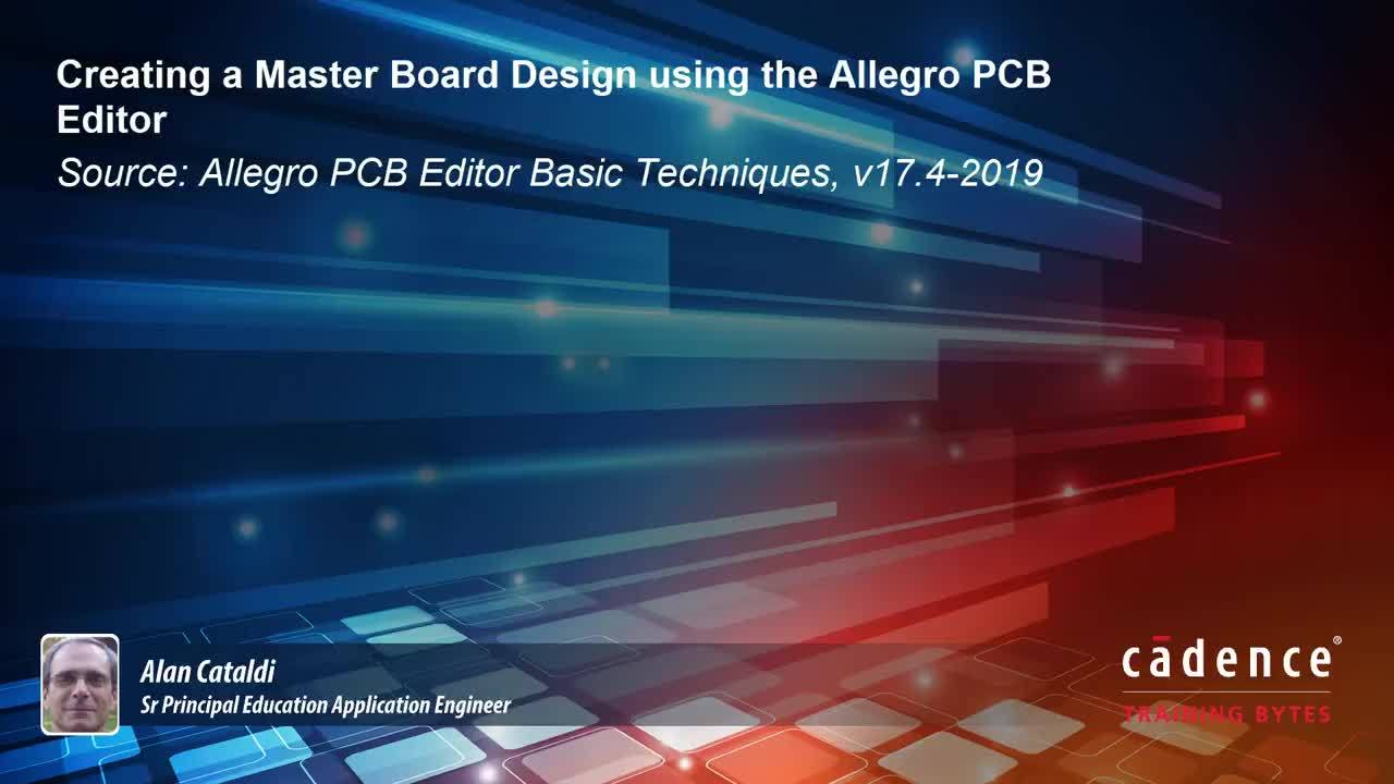
Creating A Master Board Design Using The Allegro Pcb Editor
Cadence Allegro Pcb Design Flowcad
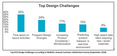
Multek Joins Cadence Designtrue Ecosystem To Deliver Pcb Design Manufacturability Earlier In The Design Process Multek

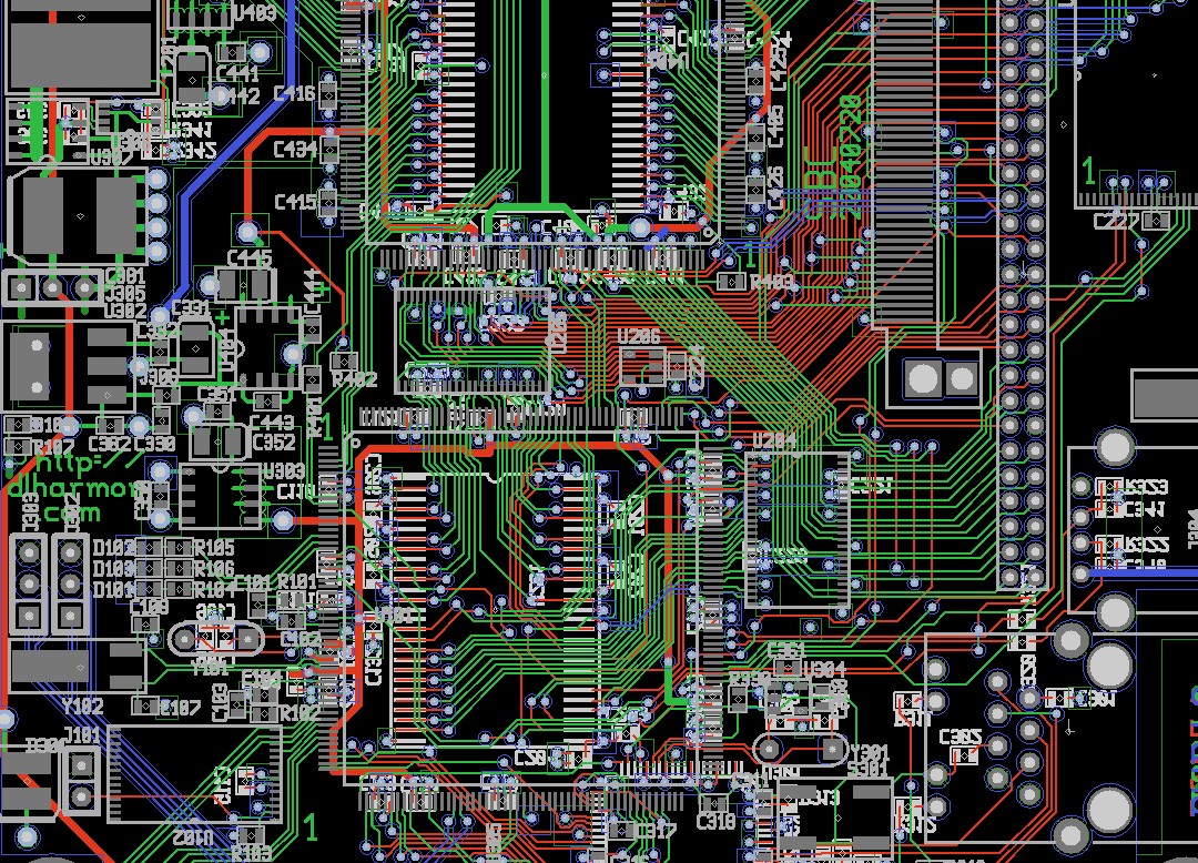
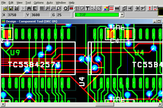
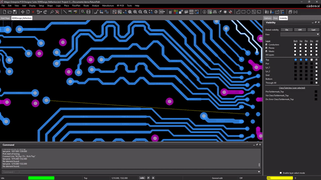
Embedded Systems Design Resources Manual Routing In Cadence Pcb Editor

Allegro Pcb Editor

Cross Probing Orcad And Allegro Inter Tool Communication Allegro Pcb Tips
High Speed Pcb Design Circuit Board Design Pcb Layout Software
Benchmark Systems
Comparing Altium And Cadence Pcb Layout Tools Hackaday
Cadence Allegro Pcb Layout Aluminum Assembly 94v0 Mp3 Buy Cadence Allegro Pcb Layout Aluminum Pcb Assembly 94v0 Mp3 Pcb Product On Alibaba Com

Ema Design Automation Announces Footprintgen An App For Cadence Allegro And Orcad Pcb Design Tools That Cuts The Time Needed To Design Pcb Footprint Models For New Components Eda360 Insider

Integration Trend Leads Pcb Design Tool Evolution Circuit Cellar
Orcad Electronic Design And Pcb Layout Flowcad
Cross Probing Intertool Communication And Pcb Design
Allegro Pcb Design 17 2 16 Pcb Design Cadence Technology Forums Cadence Community

How To Start With Cadence Allegro Very Simple Tutorial Welldone Blog
Boardsurfers Five Ways To View Your Design In 3d Canvas Pcb Design Cadence Blogs Cadence Community
(1).jpg)
עברית English Francais Espanol Russkij Homepage About Us Contact Us Trace Printed Circuit Board Design Ltd Facebook Twitter Linkedin Home About Us Welcome Products Company Profile Ytrace Pcb Types Technology Types Electronic Types
Orcad Tutorial Physical Layout Parallel Systems

Cadence Allegro Pcb Design Software Download
The Ultimate Pcb Design Software Comparison Sfcircuits

News Altium Pcb Design Software Cadence Timing Signoff Tools And More 911eda

Cadence Pcb Design Layout Pcb Circuits
Pcb Size And Shape Requirements In Circuit Board Layout Advanced Pcb Design Blog Cadence

How To Pick And Place Report By Orcad Pcb Layout Software Pcbway
How To Generate Pcb Gerber Files From Cadence Allegro Orcad The Easy Way Latest Open Tech From Seeed Studio
Cadx Services Cadence Orcad

Difference Between Native Allegro Step And Artwork S Step For Fea

Cadence Spb Allegro And Orcad V17 40 008 19 P30download

Cadence Pcb Design Analysis Linkedin

Customize Your Design Pcb Experience Orcad

Orcad Pcb Designer Suite Ema Design Automation

Design Your Electronics Schematic And Pcb Layout By Hash92
Pads P Cad Cadstar Allegro Pcb Design L Cadence
Design Pcb For You In Altium Designer Or Cadence Allegro By Zakariabelatir
Cadence Pcb Editor Suites 2 Minute Overview Orcad And Allegro Youtube

Orcad Allegro How To Edit Via Padstacks Orcad Allegro Cadence Youtube
What S Good About Allegro Pcb Editor 3d Viewing Oh My Check Out Spb16 3 Pcb Design Cadence Blogs Cadence Community

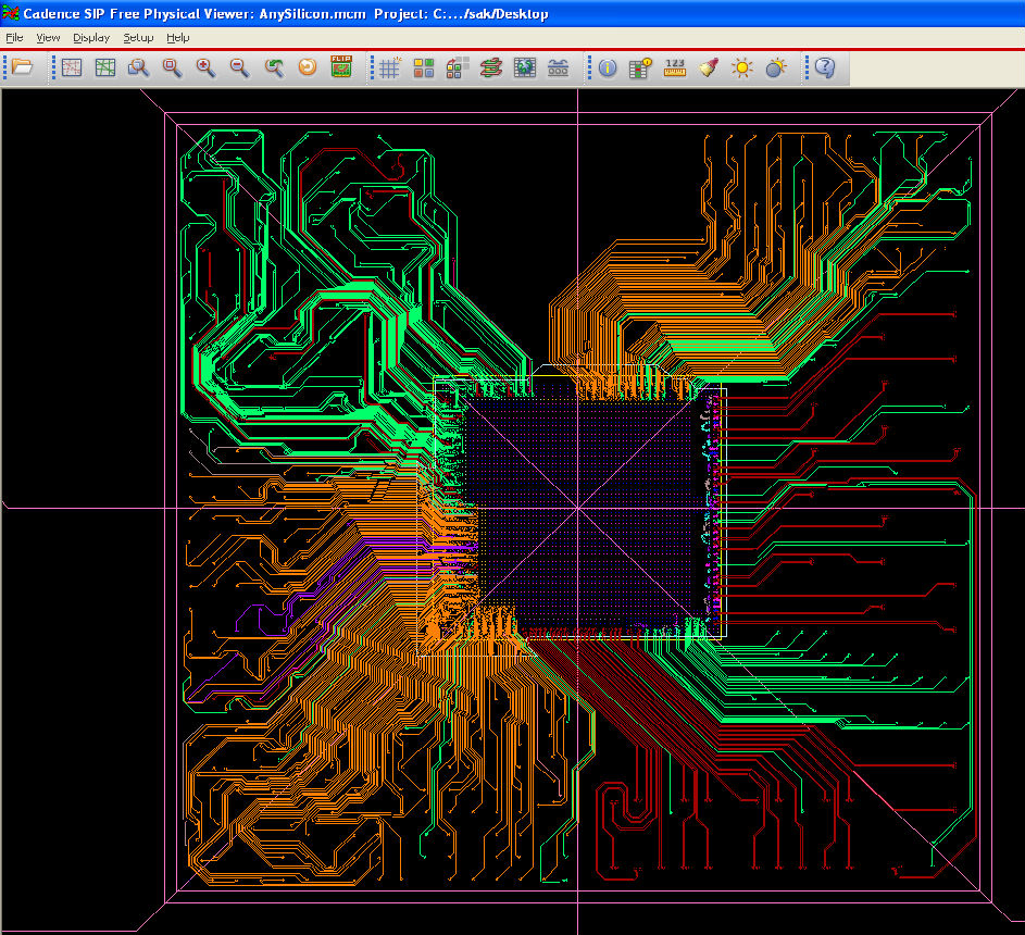
Allegro Package Designer Plus Sip Layout Option
Design Reuse Within A Pcb Layout And Beyond By Cadence Pcb Medium

Why Move Up To Allegro 17 2 16 Via Structures The Next Generation High Speed Routing Solution Reason 8 Of 10 Pcb Design Cadence Blogs Cadence Community
Allegro Pcb Designer

Customer Support Recommended Using Test Points In Allegro Design Entry Cis And Allegro Pcb Editor Flow Pcb Design Cadence Blogs Cadence Community

High Speed Pcb Board Design And Analysis
Dark Theme On Allegro Pcb Design Cadence Technology Forums Cadence Community

Pcb Layout Services Arira Design
Taking A Circuit Board Through Orcad Layout For The First Time
High Speed Pcb Board Design And Analysis

Cadence Allegro Pcb Design Solution Ftd Pcb Allegro Pcb Design Solution Allegro Pcb Designer Is A Scalable Proven Pcb Design Environment That Addresses Technological And Method Pdf Document

Cadence Pcb You Can No Longer Chuck Your Pcb Layout Into Facebook

Pcb Editor Allegro Get Distance Dimension Between Two Points Pcb Design Cadence Technology Forums Cadence Community
Allegro Import Altium Designer 21 0 User Manual Documentation

How To Start With Cadence Allegro To Set Up Parameters For Pcb Layout Advanced Pcb Design

China Shenzhen Professional Cadence Allegro Pcb Layout Design China Printed Circuit Board Professional Oem Pcb Board

Printed Circuit Boards
Orcad Allegro Pcb Design Tutorial Projectiot123 Technology Information Website Worldwide
Announcements Upverter
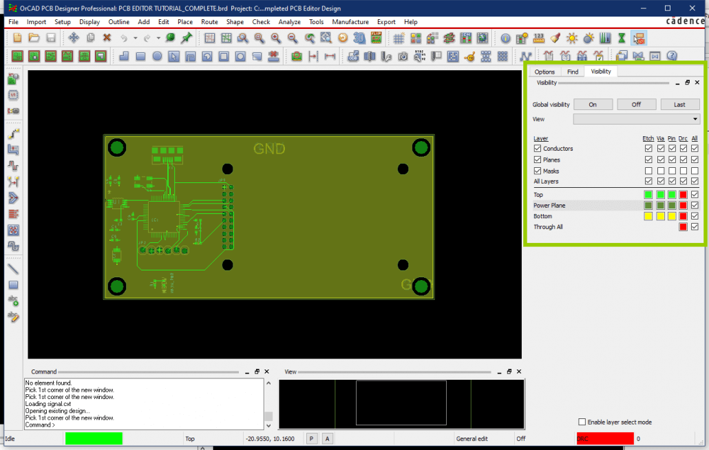
Tutorial Cadence Orcad And Allegro Pcb Editor Visibility Pane Customisation Youtube

Awr Connected Cadence Awr Software
Cadx Services Cadence Orcad
Bga Substrate Design
Outsourced Pcb Design Agencies Help You To Get Back To Design With Pcb Layout Software Of Altium Techno Faq

Pcb Layout Design In Orcad Pcb Circuits

Pcb Design Layout Your Expert For Pcb Design Service And Pcb Layout Service

Cadence Pcb Design Layout Pcb Circuits
Cadence Simulation For Pcb Design

Cadence Pcb Design Solutions Engineering Technical Pcbway

Pcb Design Layout Your Expert For Pcb Design Service And Pcb Layout Service
Pcb Design Services Magnum Technologies Pty Ltd

China Shenzhen Professional Cadence Allegro Pcb Layout Design China Printed Circuit Board Professional Oem Pcb Board

The Ultimate Pcb Design Software Comparison Sfcircuits

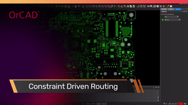
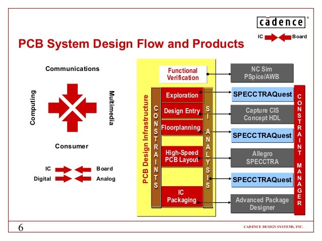
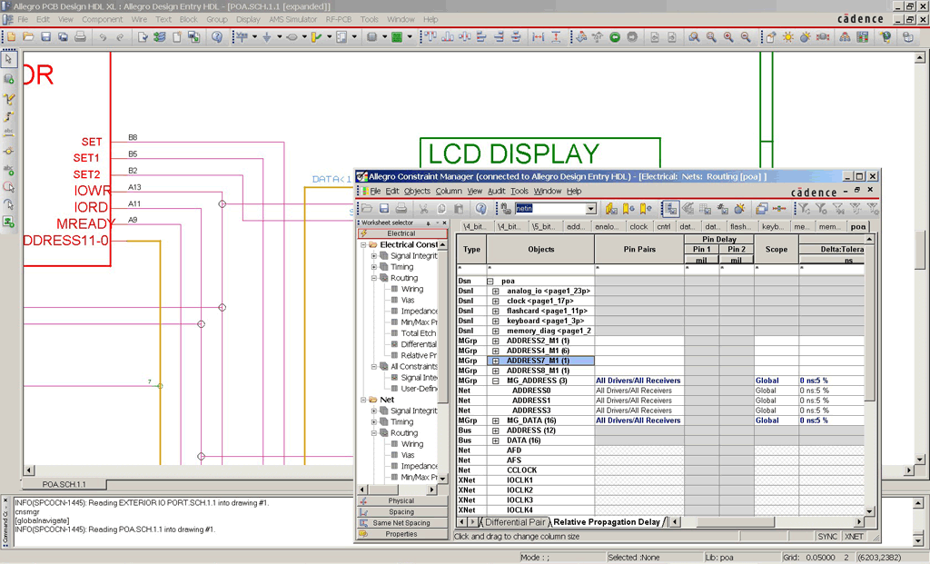
Constraint Driven Pcb Layout
Doing Pcb Layout Learn Orcad Cadence Allegro Essentials Lesson 9 Youtube

Tools Custom Electronics Design
Q Tbn And9gctylmbmpqj Rsqtvt3hdslxoc0tfsjmr48gh73xuofnzfsr0qam Usqp Cau

Rigid Flex
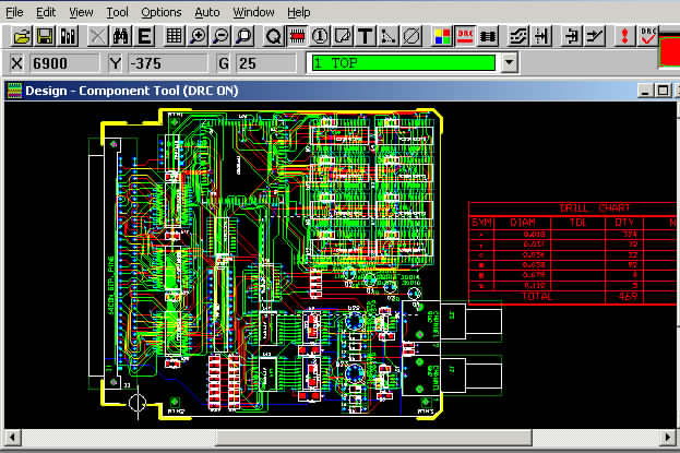
Embedded Systems Design Resources Transferring A Cadence Schematic To Pcb Editor
Q Tbn And9gcqnmxslgtvoj C7usrgizwhxhnfgon1lba2pr6u8jlq98nampir Usqp Cau
Orcad Capture 17 4 Dark Theme Pcb Design Cadence Technology Forums Cadence Community

Cadence Allegro Pcb Flow Planner Youtube Live Youtube

Cadence Allegro Pcb Design Pcbdesignservice

Allegro Downloads
Q Tbn And9gcs4qamt5fgq2omqfaqlskmnrj0srvk1b8thzvsgaextjhjqupje Usqp Cau

Allegro Pcb Editor
Orcad Tutorial Physical Layout Parallel Systems
How To Add A Company Logo Or A Marking Seregraphy With Allegro Pcb Design Pcb Design Cadence Technology Forums Cadence Community
Q Tbn And9gctvpj4onf Yc9ezfa2xlladzisp5op1hdlhuboz0ccge606vms0 Usqp Cau

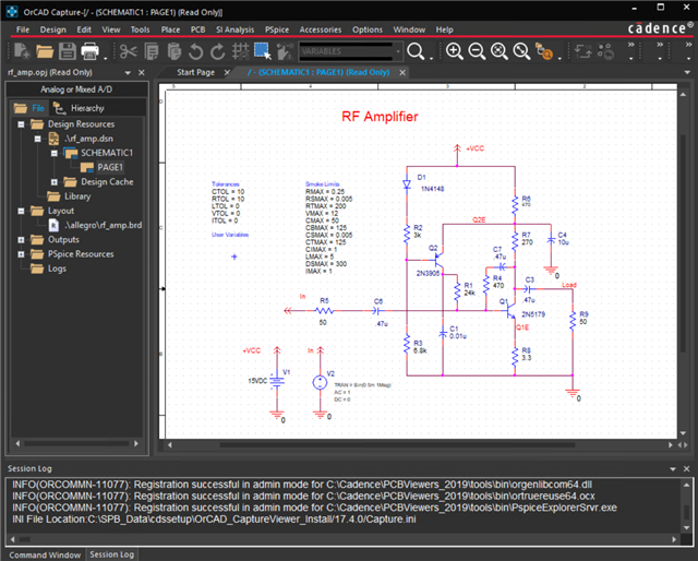
Allegro Design Entry Capture Capture Cis

Cadence Allegro Welldone Blog

News Cadence Introduces Thermal Solver For Pcb Design 911eda

Design And Library Data Management
Cfd Modeling And Simulation In Electronics Design

Allegro Pcb Designer
Quickly View Schematic Designs Boards And Ic Packages For Free Using Cadence Pcb Viewers 19 Pcb Design Cadence Blogs Cadence Community

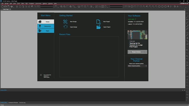
Free Orcad Trial Complete Pcb Design Solutions
Allegro Design Authoring
Pcb Layout Software Orcad Allegro Pads Cadence Pcb Design Reliable Electronics Designer Buy Pcb Layout Pcb Layout Software Reliable Electronics Designer Product On Alibaba Com
What Is A Pcb Netlist So You Ve Created A Pcb Schematic Using By Cadence Pcb Medium
Start Your First Pcb Design In Orcad


