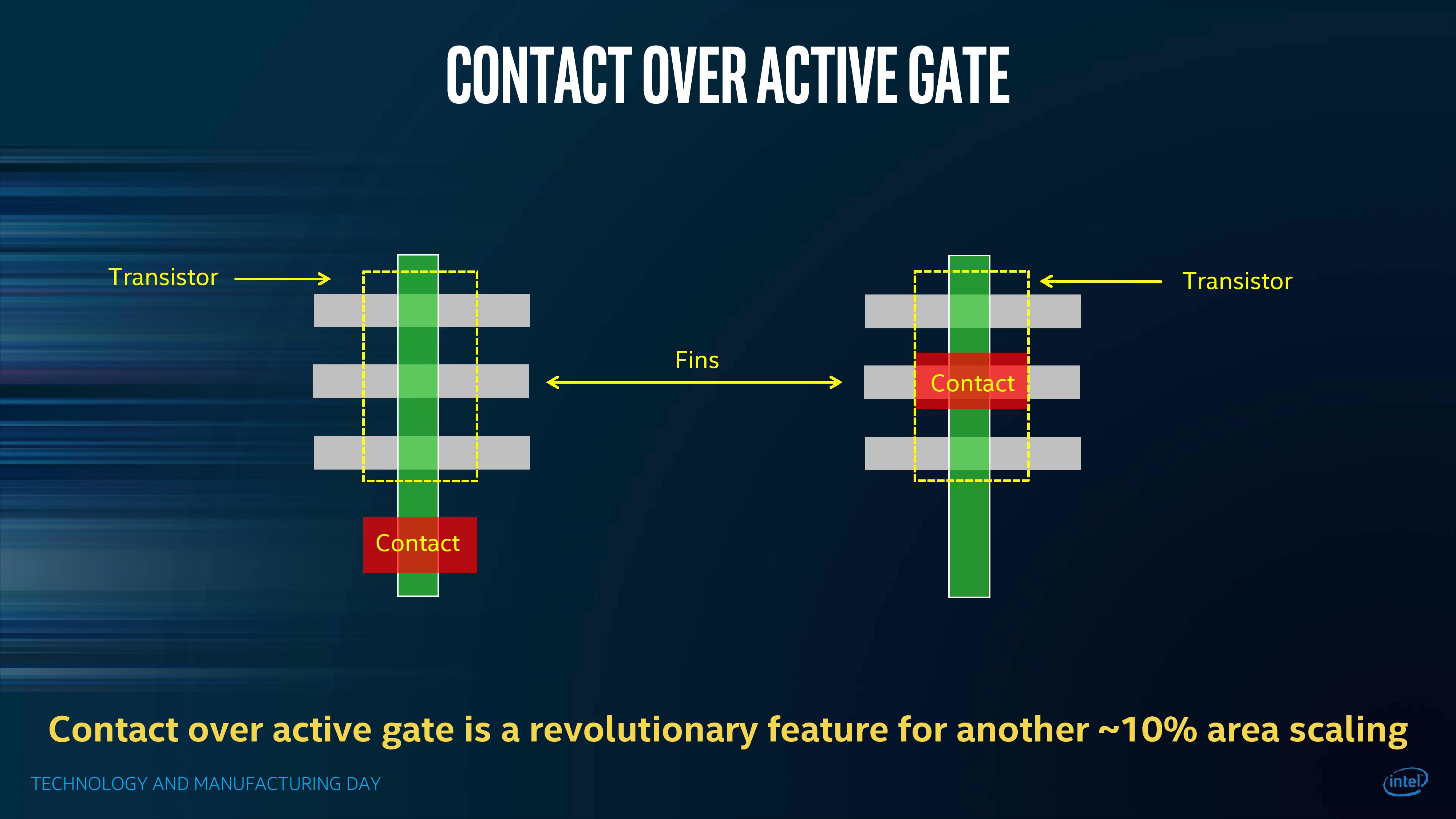
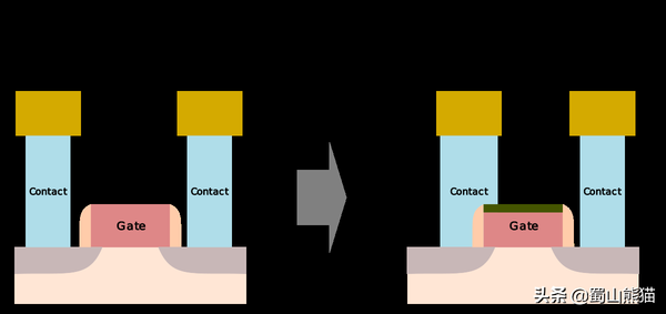
Contact Over Active Gate
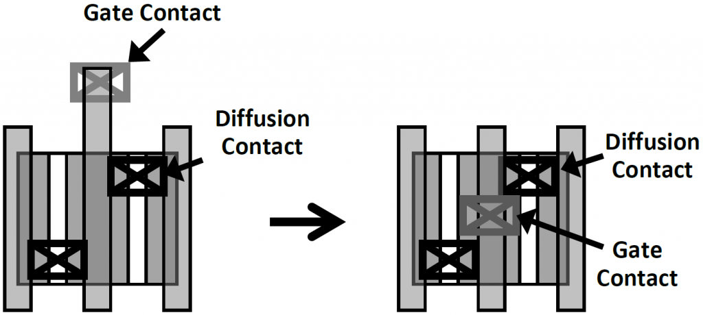
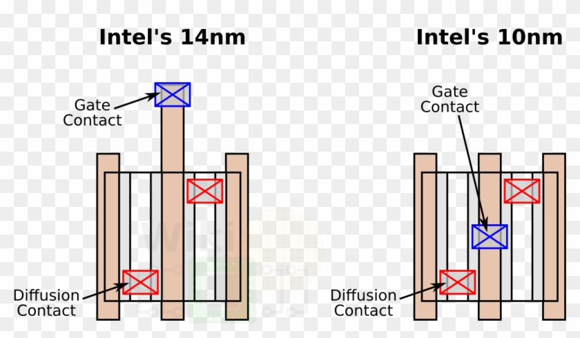
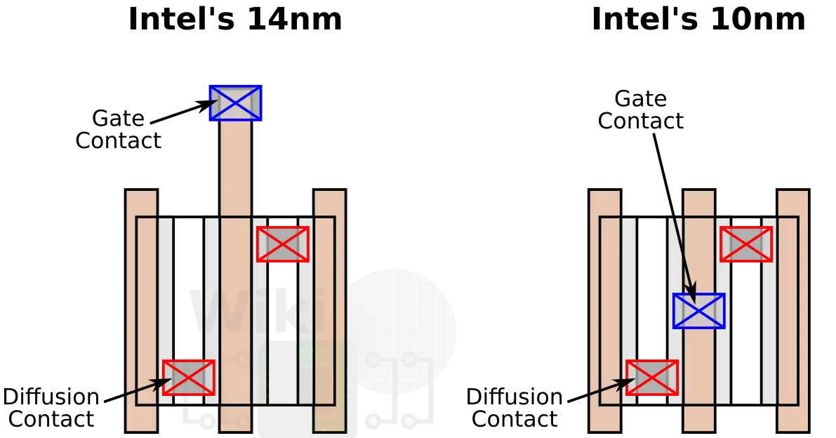
Each gate has a number of contacts used to join them to the metal layers of the chip Traditionally, the contact was offset from the gate At 10nm, Intel is stacking the contacts on top of the.
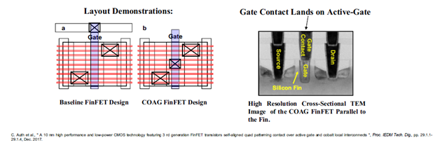
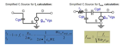
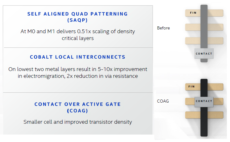
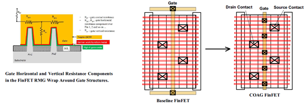
Contact over active gate. In a paper, “Improved Air Spacer CoIntegrated with SelfAligned Contact (SAC) and Contact Over Active Gate (COAG) for Highly Scaled CMOS Technology,” its researchers described how the new air spacer reduces effective capacitance – a critical factor impacting the characteristics of CMOS devices — by 15% through a reduction in the air spacer’s dielectric constant, leading to performance gains and power reductions at the same time. The second advancement is what Intel refers to as "contact over active gate," a "process feature whereby the gate contact is stacked on top of the transistor gate rather than at its side" The net. A contactoveractivegate (COAG) process step is required, as illustrated in the righthand side of the figure above Specifically, for devices used in RF circuits, the common figure of merit (FOM) is fmax, which represents the frequency at which the biased device behavior falls to unity power gain.
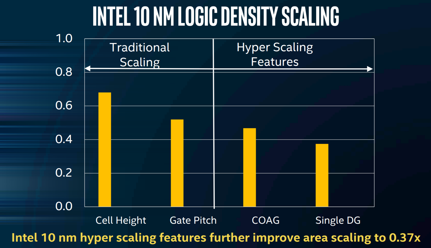
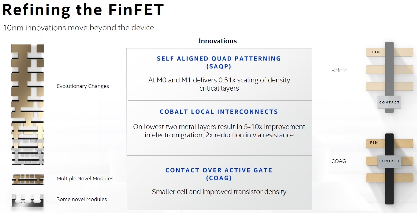
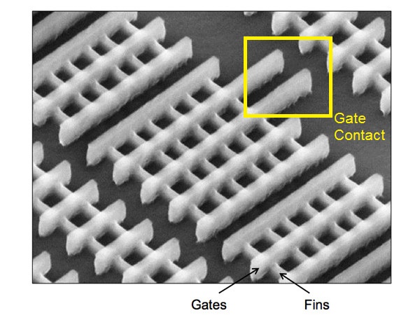
But the technology set the ground rules and a path for further innovation, its three key features — contact over active gate (COAG), usage of cobalt for local interconnects, and selfaligned quadruple patterning (SAQP) at M0 and M1 layers — are still considered as the main pillars of the whole 10nm node at large. COAG means moving the contact from a position away from the fins to directly over the active part of the CONTACT OVERACTIVE GATE Contact Contact over active gate is a revolutionary feature for another —10% area scaling We can perhaps see the concept a bit more clearly in this (somewhat fuzzy) image of 14nm transistors source/dra contacts gate. Intel has improved its 10nm scaling compared with 14nm through the use of two specific new technologies — single dummy gate, and contactoveractivegate Typically, logic cells use a pair of what.
There's also a section that mentions Intel's COAG (contact over active gate) technology, which has been rumored to have been a contributing factor in Intel's troubles with 10nm yields The video. The first of these is "contact over active gate," which means that the location where a gate crosses a fin to create a transistor is now directly over the top instead of just below it He said this. A robust gate driver can turn.
Intel’s 10nm process incorporates contact over active gate (COAG) technology, too According to Kaizad Mistry, codirector of logic technology development at Intel, moving the contact from its. Contact Over Active Gate By DeMonet (abcdelete@thisdefghi), April 13, 17 559 pm Room Moderated Discussions I was just reading through the single dummy gate thread and realized I had several questions about contact over active gate Is increased density likely the primary reason for COAG?. But the technology set the ground rules and a path for further innovation, its three key features — contact over active gate (COAG), usage of cobalt for local interconnects, and selfaligned quadruple patterning (SAQP) at M0 and M1 layers — are still considered as the main pillars of the whole 10nm node at large.
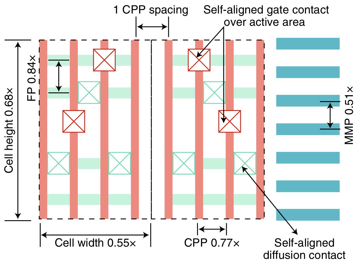
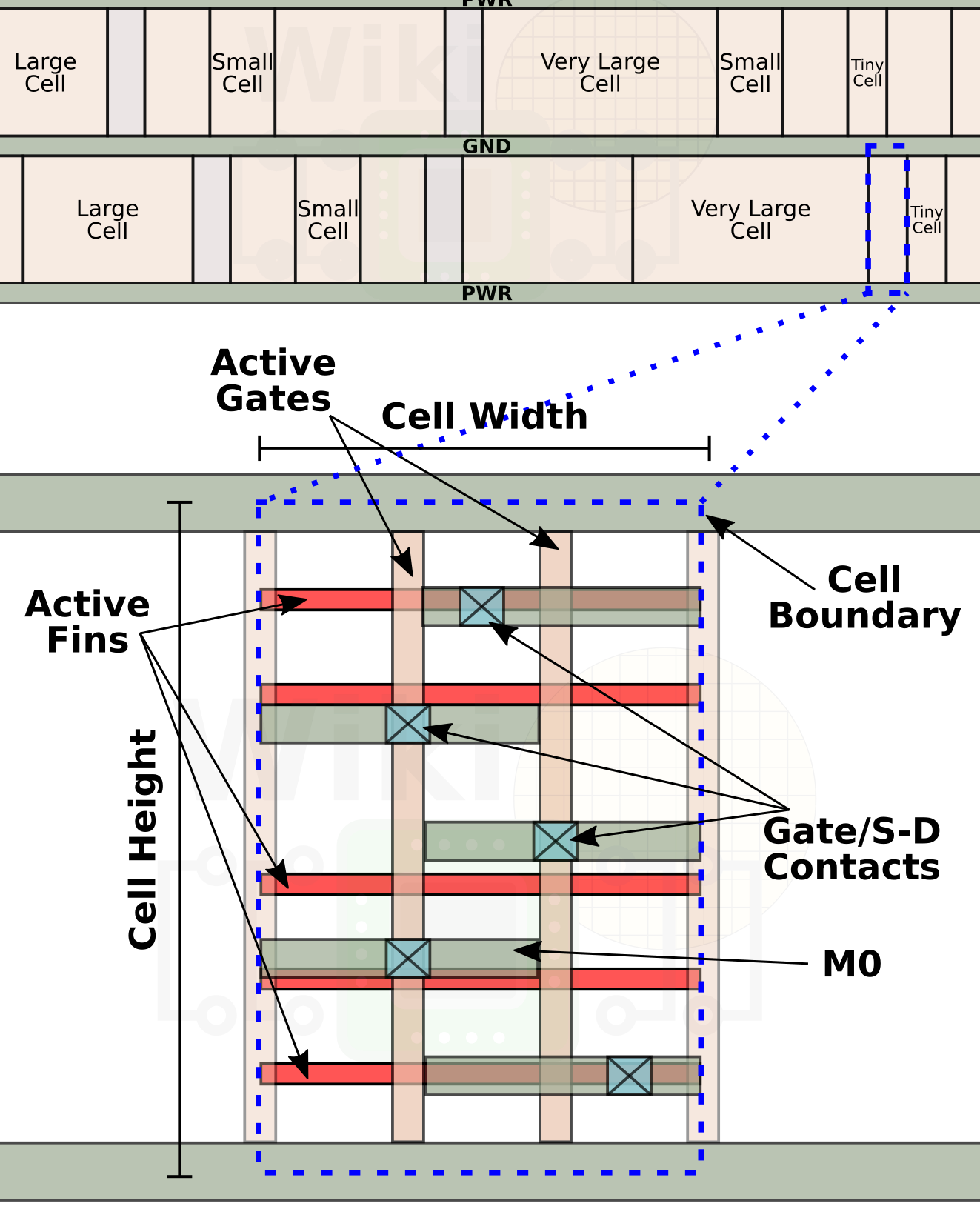
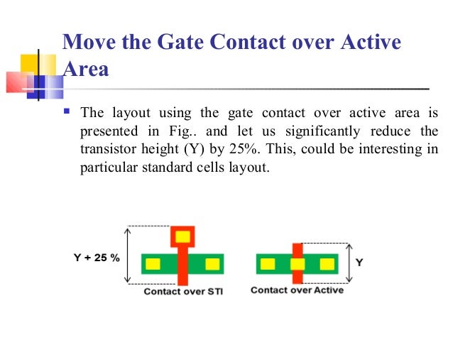
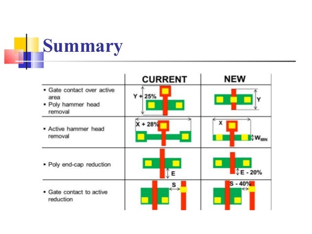
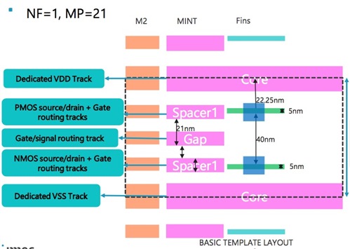
That also assumes gatecontactoveractive, which allows one fin spacing between NMOS and PMOS, and two shared fin spacings separating the cells above and below 175/7 gives a 25nm fin pitch, a 17% shrink, and doable with SAQP or EUV. However, I think there were 2 different Intel 10nm nodes The first was used on Cannonlake and yielded very badly The second updated version is used for Ice lake, but they had to remove COAG (Contact Over Active Gate) and also relax the metal pitch to 40nm in order to get it yield properly. Move the Gate Contact over Active Area The layout using the gate contact over active area is presented in Fig and let us significantly reduce the transistor height (Y) by 25% This, could be interesting in particular standard cells layout.
Cobalt Interconnect (M0, M1) 1st Gen Foveros 3D Stacking;. Contact over active gate (COAG), and single dummy gate (SDG), which in total are claimed to add another 30% transistor density improvement COAG means moving the contact from a position away from the fins to directly over the active part of the gate. History and shipping volumes decisively validated the gatelast model From there, the video spends time discussing both FinFETs and Contact Over Active Gate (COAG), the new technology Intel.
The Intel Ice LakeSP lineup would be directly competing against. Embodiments of the present disclosure provided herein generally include a device and method of forming a device that has an improved gate contact structure that is formed over active regions of a semiconductor device In some embodiments, the improved gate contact structure is a selfaligned contact gate formed in a patterned contact via opening. Intel tells us that its currentlyshipping version of 10nm still uses Cobalt, Contact Over Active Gate (COAG), and SelfAligned Quad Patterning (SAQP) This trio of new technologies enabled a 27X.
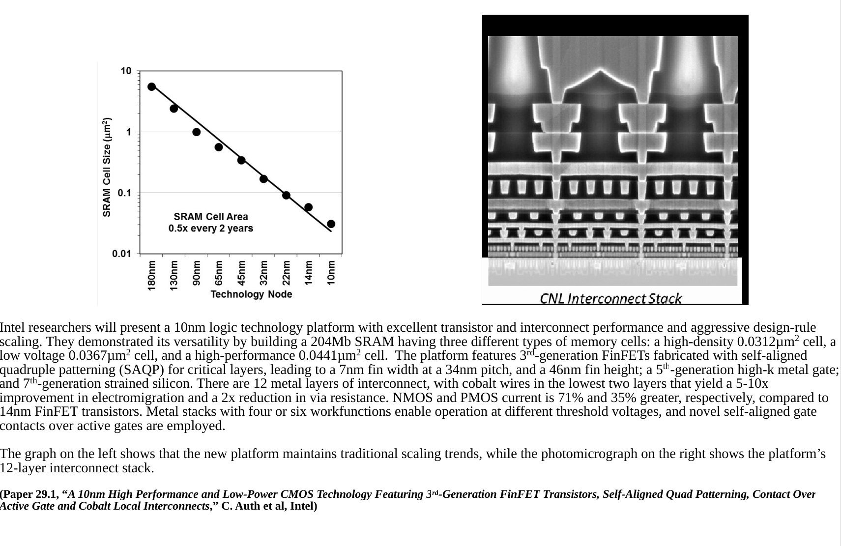
Intel Xeon Roadmap Leaked Out, Unveils 10nm Ice LakeSP With PCIe Gen 4 & Up To 26 Cores in , NextGen Sapphire Rapids With PCIe Gen 5 & DDR5 in 21. For high density, a novel selfaligned contact over active gate process and elimination of the dummy gate at cell boundaries are introduced The transistors feature rectangular fins with 7nm fin width and 46nm fin height, 5 th generation highk metal gate, and 7 th generation strained silicon. DeMonet (abcdelete@thisdefghi) on April 13, 17 659 pm wrote > I was just reading through the single dummy gate thread and realized > I had several questions about contact over active gate.
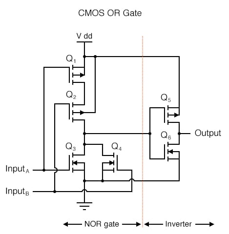
Contact over active gate is a revolutionary feature for another ~10% area scaling Transistor Contact Contact Over Active gate Transistor Fins Contact Gate Gate TECHNOLOGY AND MANUFACTURING DAY Single dummy Gate 14 nm 10 nm Single Dummy Gate Active Gate Active Gate Dummy Gates. Gateoxide Tungsten TiSi 2 DualWell TrenchIsolated CMOS Process Contact To Poly Contact To Diffusion Via Well (p,n) Active Area (n,p) Color Representation Yellow Green Red Blue Magenta Black Black Black Select (p,n) Green Digital Integrated Circuits Manufacturing Process EE141. Gateoxide Tungsten TiSi 2 DualWell TrenchIsolated CMOS Process Contact To Poly Contact To Diffusion Via Well (p,n) Active Area (n,p) Color Representation Yellow Green Red Blue Magenta Black Black Black Select (p,n) Green Digital Integrated Circuits Manufacturing Process EE141.
Contact over active gate (COAG) is a novel design trick that allows the placement of gate contacts directly on the top of active transistor regions 17, thus reducing the standard cell size In. Cobalt Interconnect (M0, M1) 1st Gen Foveros 3D Stacking;. A gate structure is formed over the channel region, and the gate structure includes a HKMG and airgap spacers formed on opposite sidewalls of the HKMG Each of the airgap spacers includes an air gap that is formed along a trench silicide region, and the airgap is formed below a top of the HKMG A gate contact is formed over the active region.
And now the gate contact can be placed atop the gate (“contact over active gate”) that achieves a 10% area savings versus prior nodes’ alongsidethegate. Gateoxide Tungsten TiSi 2 DualWell TrenchIsolated CMOS Process Contact To Poly Contact To Diffusion Via Well (p,n) Active Area (n,p) Color Representation Yellow Green Red Blue Magenta Black Black Black Select (p,n) Green Digital Integrated Circuits Manufacturing Process EE141. In addition to the feature shrinks, there are technology changes in the standard cell layout The dummy gates at the cell boundaries have gone, replaced by a single gate spacing;.
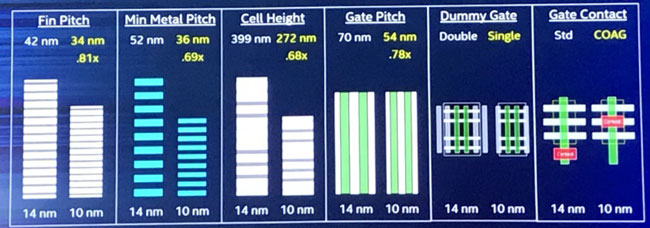
Beyond lithography, the third generation FinFET transistors themselves are taller (54 nm) and narrower (34 nm pitch), as compared to 42×42 nm in 14 nm, and 34×60 nm in 22 nm;. Contact over active gate Semiconductors Further Industry Thoughts on FullNodes, InterNodes, LeadingNodes and TrailingNodes – Part 2 by Sundeep Bajikar May 29, 18 Part 2 of my blog series looks at how new materials, materials engineering and 3D design techniques are extending the semiconductor technology roadmap even as classic 2D. Contact over active gate Semiconductors Further Industry Thoughts on FullNodes, InterNodes, LeadingNodes and TrailingNodes – Part 2 by Sundeep Bajikar May 29, 18 Part 2 of my blog series looks at how new materials, materials engineering and 3D design techniques are extending the semiconductor technology roadmap even as classic 2D.
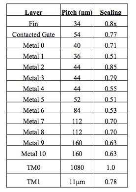
Another scaling booster is contactoveractivegate (COAG), see the image to the top left The metal stack has two layers of Cobalt and 10 layers of copper Above are the widths and spacings of each layer The scaling numbers are with respect to the prior 14nm node. A gate contact structure is disposed on the portion of the gate structure disposed above the active region of the substrate Gate contact structures disposed over active portions of gates and. Or would it likely have other benefits?.
This is a 10 nm technology featuring the third generation of Intel's FinFETs, seventh generation of strained silicon, fifth generation of highk metal gate, multiVt options, contact over active gate, singlegate isolation, 14 metal layers, lowk interlayer dielectric, multiplate metalinsulatormetal capacitors, two thickmetal routing layers for lowresistance power routing, and leadfree packaging. Or would it likely have other benefits?. Contact Over Active Gate;.
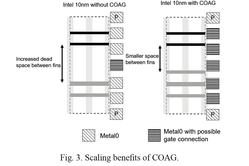
291 A 10nm High Performance and LowPower CMOS Technology Featuring 3rd Generation FinFET Transistors,SelfAligned Quad Patterning,Contact over Active Gate and Cobalt Local Interconnects Created Date 1/18/18 PM. Activeclamp reset With sufficiently fast gate drive, the turn off of Q1 can be virtually lossless To accomplish this, the gate of Q1 must be turned off (and the flow of current stopped) before the drain voltage has a chance to rise The rise of the drain voltage is delayed due to the drainsource capacitance;. Another recent scaling booster comes in the form of contactoveractivegate, also known as selfaligned gate contacts Traditionally there has been deadspace within the cell as the gate contact had to be dropped away from the active areas of the cell — this kept the cell height from shrinking as much as desired.
Contact Over Active Gate;. Two other elements of the hyper scaling were also detailed;. In technologies where contacting poly over active is prohibited, it is this portion of the poly "field poly" ("POLY NOT ACTIVE" in SVRF language) where the gate contact should land on Gate contact over active is used not only in the latest FinFET technologies, but also in old technologies where density is of primary importance eg, in image sensor designs (CMOS image sensors), that use quite old technologies 180nm, 130nm, 90nm, etc.
A gate contact structure is disposed on the portion of the gate structure disposed above the active region of the substrate Gate contact structures disposed over active portions of gates and. Intel Xeon Roadmap Leaked Out, Unveils 10nm Ice LakeSP With PCIe Gen 4 & Up To 26 Cores in , NextGen Sapphire Rapids With PCIe Gen 5 & DDR5 in 21. Heathergate at Oxford Valley is a 55 community that boasts 17 gorgeous green acres conveniently situated in Lower Bucks County This exceptional locale makes it an ideal setting for active adults seeking a lifestyle that offers all of the bells and whistles without the everyday hassles of homeownership.
And the gate contact is now over the active gate, ending the need for isolation space to fit in the contact. Contact Over Active Gate (COAG) Within a transistor, the gate contact is the control point where the current for the gate is applied to control between the source and the drain sides of the fin. A gate contact structure is disposed on the portion of the gate structure disposed above the active region of the substrate Gate contact structures disposed over active portions of gates and.
#IEDM17 Highlight Paper 291 “A 10nm High Performance and LowPower CMOS Technology Featuring 3rdGeneration FinFET Transistors, SelfAligned Quad Patterning, Contact Over Active Gate and. COAG (contact over active gate) – A process feature whereby the gate contact is stacked on top of the transistor gate rather than at its side Intel has implemented COAG in its 10nm process – an industry first – thereby improving transistor density CPT (cost per transistor). Contact Over Active Gate By DeMonet (abcdelete@thisdefghi), April 13, 17 559 pm Room Moderated Discussions I was just reading through the single dummy gate thread and realized I had several questions about contact over active gate Is increased density likely the primary reason for COAG?.
And now the gate contact can be placed atop the gate (“contact over active gate”) that achieves a 10% area savings versus prior nodes’ alongsidethegate. Embodiments of the present disclosure provided herein generally include a device and method of forming a device that has an improved gate contact structure that is formed over active regions of a semiconductor device In some embodiments, the improved gate contact structure is a selfaligned contact gate formed in a patterned contact via opening. The first of these is "contact over active gate," which means that the location where a gate crosses a fin to create a transistor is now directly over the top instead of just below it He said this.
32a Spacing to poly over active 100 33 Gate extension beyond active 100 34 Active extension beyond poly 100 35 Spacing of poly to active 70 41 Spacing from substrate/well to gate 150 42 Overlap by poly or active 1 43 Overlap of substrate/well contact 1 44 Spacing to select 0 Well Active (diffusion) Poly (ie.
Gate Control Theory Wikipedia

Chip Variability Mitigation Through Continuous Diffusion Enabled By Euv And Self Aligned Gate Contact Semantic Scholar

Claimparse
Contact Over Active Gate のギャラリー

Usb2 Transistor With Contact Over Gate Active Area Google Patents
Igbts Frequently Asked Questions Faqs Power Electronics
Docs Broadcom Com Doc Av02 4977en

Intel Shows How A 10nm Processor Goes From Sand To Silicon

Usb2 Gate Contact Structure Over Active Gate And Method To Fabricate Same Google Patents
Nature Electronics News Views Suman Datta Analyses Intel S 10 Nanometre Cmos Logic Technology Which Delivers 100 Million Transistors Per Square Millimetre T Co Asd5i1w5g7 T Co Perzkdw9jg
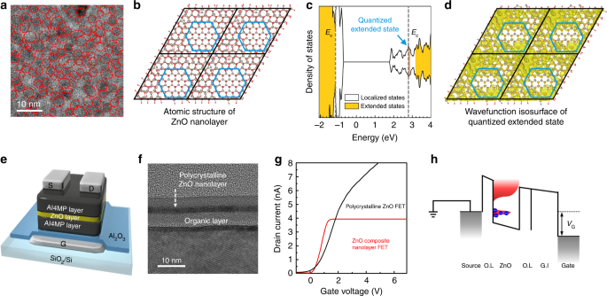
Zno Composite Nanolayer With Mobility Edge Quantization For Multi Value Logic Transistors Nature Communications
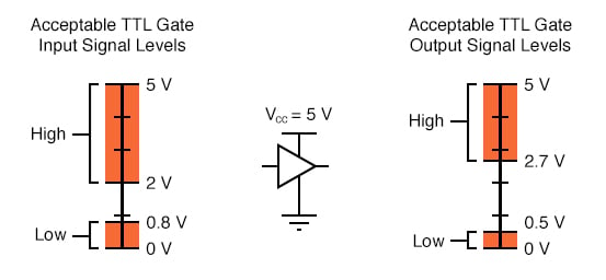
Logic Signal Voltage Levels Logic Gates Electronics Textbook
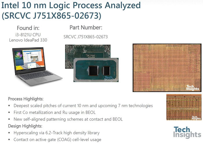
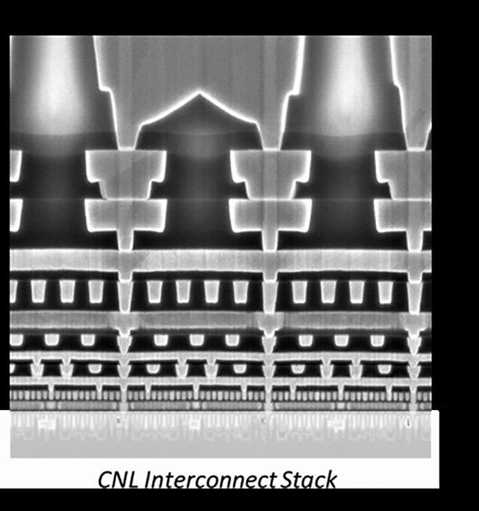
Iedm 17 Isscc 18 Intel S 10nm Switching To Cobalt Interconnects Page 4 Wikichip Fuse

How Bill And Melinda Gates Are Transforming Life For Billions In The 21st Century Fortune
Life At 10nm Or Is It 7nm And 3nm Eejournal

Intel Acknowledges It Was Too Aggressive With Its 10nm Plans Extremetech
Intel Introduced The Finfet Process Technology With The Norms Of 10 Nm And 22 Nm

Intel Architecture Day Tiger Lake Xe And Superfin Pc Perspective
Gate Driver Ics Infineon Technologies
Intel 10nm 7nm Cpu Gpu Rumor Thread Cannonlake Icelake Tigerlake Sapphire Rapids Etc H Ard Forum
Optimazation Of Standard Cell Layout
Intel 10nm Density Is 2 7x Improved Over Its 14nm Node Cpu News Hexus Net
2
Aip Scitation Org Doi Pdf 10 1063 1
Aip Scitation Org Doi Pdf 10 1063 1

Layout Optimizations To Decrease Internal Power And Area In Digital Cmos Standard Cells Semantic Scholar
Pubs Acs Org Doi Pdf 10 1021 Acs Chemmater 0c
Small Contact Resistance And High Frequency Operation Of Flexible Low Voltage Inverted Coplanar Organic Transistors Nature Communications

Insulated Gate Bipolar Transistor Or Igbt Transistor

Study Of Gate Contact Over Active Area Semantic Scholar
Ieeexplore Ieee Org Iel7 4 Pdf
Aip Scitation Org Doi Pdf 10 1063 1
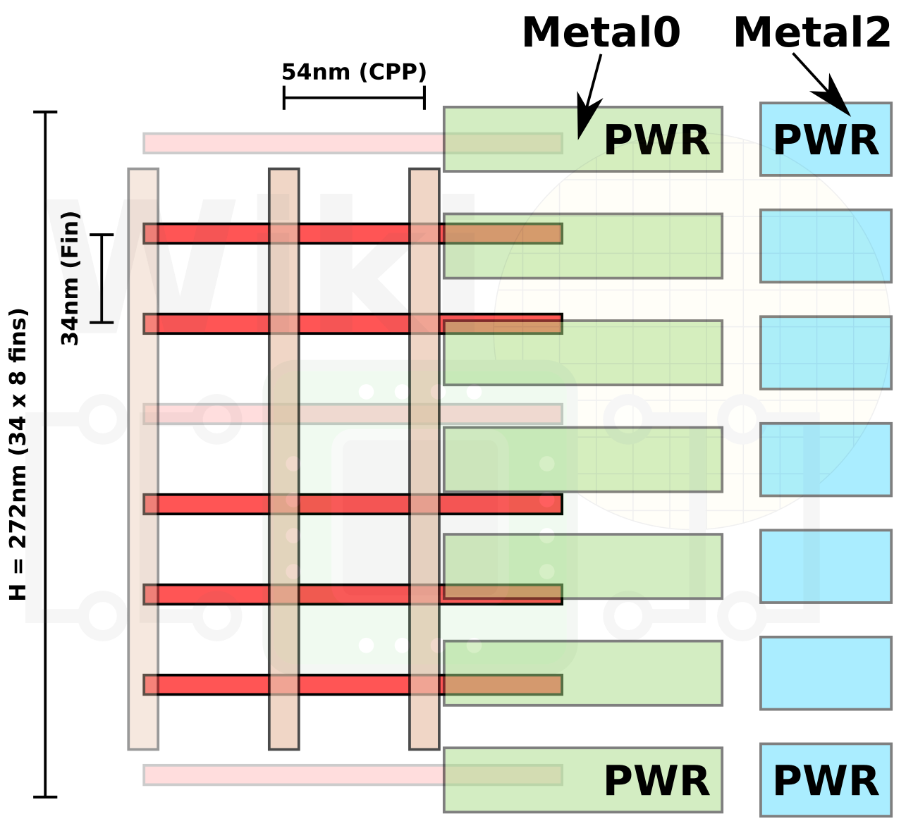
Iedm 18 Intel S 10nm Standard Cell Library And Power Delivery Wikichip Fuse
Http Ieeexplore Ieee Org Iel7 601 Pdf

Bald Engineering Born In Finland Born To Ald Intel To Present 10 Nm Logic With 3rd Gen Finfet And 2 Level Cobalt Interconnect
Contact Over Active Gate Process Requirements For 5g Semiwiki

New Gaa Nanosheet Architecture To Drive Silicon Performance Ee Times Asia

Intel Unveils More 10nm Details By Dick James By Eray Hsieh Medium
Optimazation Of Standard Cell Layout
Bald Engineering Born In Finland Born To Ald Intel To Present 10 Nm Logic With 3rd Gen Finfet And 2 Level Cobalt Interconnect

Study Of Gate Contact Over Active Area Semantic Scholar
Cmos Gate Circuitry Logic Gates Electronics Textbook
Http Ieeexplore Ieee Org Iel7 601 Pdf

Figure 3 From A 23 6 Mb Mm 2 Sram In 10 Nm Finfet Technology With Pulsed Pmos Tvc And Stepped Wl For Low Voltage Applications Semantic Scholar
Pdfs Semanticscholar Org 2f16 Cbe4e52fdd6bc7a3225bf32e39 Pdf
Intel 10nm Superfin Technology Read More On Semiwiki
Irds Ieee Org Images Files Pdf 17 17irds Mm Pdf
Cmos Gate Circuitry Logic Gates Electronics Textbook
Optimazation Of Standard Cell Layout
Q Tbn And9gcrjptsh9klrelh7hyke1tsxnf0kclmes77fv8yyonyvuusndnku Usqp Cau
Gate Driver Ics Infineon Technologies
Intel S 10nm Cannon Lake Silicon Design Intel S 10nm Cannon Lake And Core I3 8121u Deep Dive Review
3nm Cadence And Imec Breakfast Bytes Cadence Blogs Cadence Community

Intel Confirms 10nm In 19 7nm In 21 First Xe 7nm Gpus In 21
Http Ieeexplore Ieee Org Iel7 601 Pdf
Http Ieeexplore Ieee Org Iel7 601 Pdf
Http Ieeexplore Ieee Org Iel7 601 Pdf
Intel S Coag Process Contact Over Active Gate Clipart Pikpng
Http Ieeexplore Ieee Org Iel7 601 Pdf
Cmos Gate Circuitry Logic Gates Electronics Textbook

Usa1 Gate Contact Structure Over Active Gate And Method To Fabricate Same Google Patents

Active Gate Driving Technique For A 10 V Sic Mosfet To Minimize Detrimental Effects Of Parasitic Inductance In The Converter Layout Semantic Scholar
Aip Scitation Org Doi Pdf 10 1063 1
Http Ieeexplore Ieee Org Iel7 601 Pdf

17 Manufacturing Day Archives Webdomino Net

Usb2 Gate Contact Structure Over Active Gate And Method To Fabricate Same Google Patents
Contact Over Active Gate Process Requirements For 5g Semiwiki
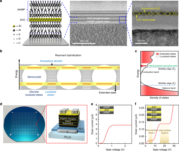
Zno Composite Nanolayer With Mobility Edge Quantization For Multi Value Logic Transistors Nature Communications
Intel S 10nm Cannon Lake Silicon Design Intel S 10nm Cannon Lake And Core I3 8121u Deep Dive Review

Pdf Active Gate Control For Current Balancing Of Parallel Connected Igbt Modules In Solid State Modulators Semantic Scholar

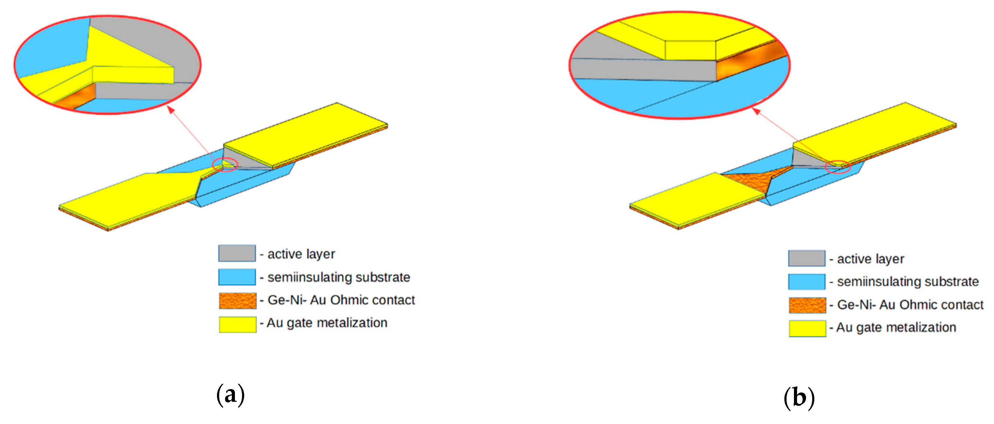
Pdf Finfet With Contact Over Active Gate For 5g Ultra Wideband Applications
Contact Over Active Gate Process Requirements For 5g Semiwiki
Cmos Gate Circuitry Logic Gates Electronics Textbook
Http Ieeexplore Ieee Org Iel7 601 Pdf

Mosfet Modeling Aimed At Minimizing Emi In Switched Dc Dc Converters Using Active Gate Control Semantic Scholar
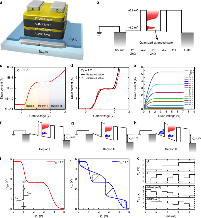
Zno Composite Nanolayer With Mobility Edge Quantization For Multi Value Logic Transistors Nature Communications

A Reliability Overview Of Intel S 10 Logic Technology Semantic Scholar

Study Of Gate Contact Over Active Area Semantic Scholar

Intel Acknowledges It Was Too Aggressive With Its 10nm Plans Bizwhiznetwork Com Innovation Li
Http Ieeexplore Ieee Org Iel7 601 Pdf

Summary Of Intel S Latest Product Roadmap Thakoni

Usb2 Gate Contact Structure Over Active Gate And Method To Fabricate Same Google Patents

Usb2 Gate Contact Structure Over Active Gate And Method To Fabricate Same Google Patents
A Super Technology Mid Life Kicker For Intel Semiwiki
Iedm 17 Isscc 18 Intel S 10nm Switching To Cobalt Interconnects Page 4 Wikichip Fuse
Contact Over Active Gate Process Requirements For 5g Semiwiki
Http Ieeexplore Ieee Org Iel7 601 Pdf
Ieee Iedm Iedm17 Highlight Paper 29 1 A 10nm High Performance And Low Power Cmos Technology Featuring 3rd Generation Finfet Transistors Self Aligned Quad Patterning Contact Over Active Gate And Cobalt Local Interconnects C

Ieee Iedm Iedm17 Highlight Paper 29 1 A 10nm High Performance And Low Power Cmos Technology Featuring 3rd Generation Finfet Transistors Self Aligned Quad Patterning Contact Over Active Gate And Cobalt Local Interconnects C

Contact Over Active Gate Applied Materials Blog

The Race To 10 7nm

Study Of Gate Contact Over Active Area Semantic Scholar
Intel给tiger Lake用的10nm超级finfet 超级在哪里 比台积电5nm还强 知乎

Tutorial 4 Designing In Advanced Technologies A Quick Review Of Approaches Pdf Free Download

Double Gate Latches 360 Yardware
Sensors Free Full Text Gated Bow Tie Diode For Microwave To Sub Terahertz Detection Html

Intel Acknowledges It Was Too Aggressive With Its 10nm Plans Extremetech
2
画像 後藤弘茂のweekly海外ニュース Intelの次世代cpuマイクロアーキテクチャ Sunny Cove 5 6 Pc Watch
Iedm 18 Intel S 10nm Standard Cell Library And Power Delivery Page 2 Wikichip Fuse
Intel 10nm Breakfast Bytes Cadence Blogs Cadence Community
3nm Cadence And Imec Breakfast Bytes Cadence Blogs Cadence Community


